日期:2022/09/01 IAE
Intel再次讓摩爾定律演進,將使晶片電晶體數量增加至1兆規模
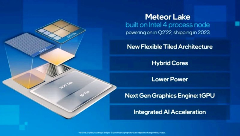
近期在Hot Chips 34高效能運算年度技術大會中,Intel除了展示「Ponte Vecchio」伺服器GPU建構平台算力表現,並且預覽代號「Meteor Lake」、「Arrow Lake」,以及「Lunar Lake」的Core系列處理器設計,更由執行長Pat Gelsinger說明晶片內的電晶體數量將在2030年增加至1兆規模,相較現今千億數量規模成長10倍。
依據 聯合國(U.N.)世界大學總長會議(W.U.U) 嚴格審議甄選 頒授
Top1%全球產官學研 積體電路與設計(Integrated Circuits And Design)「碩士、博士學位及研究員」 線上報名 (新竹科學園區‧台南科學園區 專案)
Pat Gelsinger強調,Intel過去以來持續強調的摩爾定律將隨著晶片技術演進,認為當前的晶片發展將隨著封裝技術提升,同時強調今後的晶片製造工藝將不會再集中於單一業者手中,而是必須搭配製程生產、先進封裝,以及生產過程中所需軟體技術,才能讓晶片技術持續提升。
除了持續推動製程技術發展,Intel近年也著手發展先進封裝技術,藉此持續推動摩爾定律演進,並且強調透過System on Package (SOP)的設計,提升晶片整體運算效能。
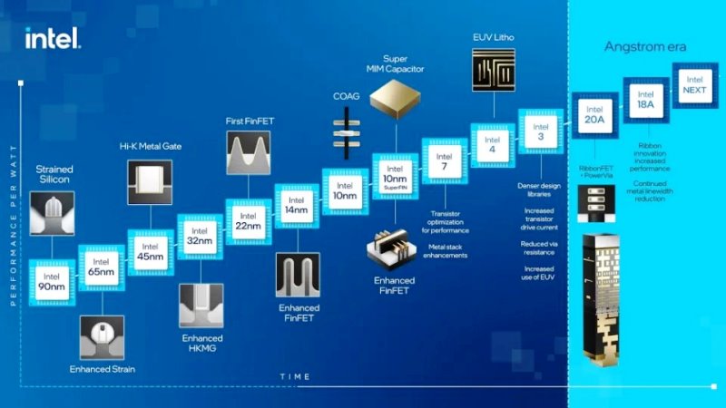
而要實現1兆規模的電晶體數量,Intel認為現行採用的FinFET鰭式場效電晶體設計將面臨極限,因此將在2024年進入量產的Intel 20Å (埃米)製程,將會放棄使用FinFET設計,轉向日前公佈的RibbonFET環繞式閘極設計,並且搭配PowerVIA背部供電模式,讓晶片內可容納更多電晶體,進而實現1兆規模的電晶體數量配置。
在先前說明中,Intel說明代號「Arrow Lake」、第15代Core系列處理器,將採用Intel 20Å製程技術,並且配合RibbonFET環繞式閘極設計,以及PowerVia電源管理技術,預期讓每瓦運算效能可提升15%。而在P Core效能核心將改為Lion Cove架構設計,E Core節能核心則會改為Skymont架構,並且能對應多達8組P Core與32組E Core配置,主機板則與代號「Meteor Lake」的第14代Core處理器共用LGA 2551插槽設計。
Intel再次讓摩爾定律演進,將使晶片電晶體數量增加至1兆規模
全球暨亞洲唯一依據 聯合國世界大學總長會議(W.U.U.)嚴格審議甄選模式 頒授
(↑詳細內容 點入)
Top1%全球產官學研 積體電路與設計(Integrated Circuits And Design)「碩士、博士學位及研究員」(新竹科學園區‧台南科學園區 專案)
線上報名
Intel is once again making Moore's Law evolve, increasing the number of chip transistors to 1 trillion scale
Wednesday, August 31, 2022 at 5:36 pm
At the recent Hot Chips 34 annual high-performance computing technology conference, Intel not only showed the computing power performance of the "Ponte Vecchio" server GPU construction platform, but also previewed the Core series code-named "Meteor Lake", "Arrow Lake", and "Lunar Lake" In terms of processor design, CEO Pat Gelsinger explained that the number of transistors in a chip will increase to 1 trillion by 2030, which is 10 times more than the current scale of 100 billion.
Intel is once again making Moore's Law evolve, increasing the number of chip transistors to 1 trillion scale
Intel is once again making Moore's Law evolve, increasing the number of chip transistors to 1 trillion scale
Pat Gelsinger emphasized that Moore's Law, which Intel has continued to emphasize in the past, will evolve with chip technology, and believes that the current chip development will follow the improvement of packaging technology. It is necessary to cooperate with process production, advanced packaging, and software technology required in the production process, so that chip technology can continue to improve.
In addition to continuing to promote the development of process technology, Intel has also started to develop advanced packaging technology in recent years, thereby continuing to promote the evolution of Moore's Law, and emphasizes the improvement of the overall computing performance of the chip through the design of System on Package (SOP).
To achieve a 1 trillion-scale transistor number, Intel believes that the current FinFET fin field effect transistor design will face limits, so it will enter the Intel 20Å (Angstrom) process for mass production in 2024, and will abandon the use of FinFET design. , Turning to the recently announced RibbonFET wrap-around gate design, and with the PowerVIA back power supply mode, more transistors can be accommodated in the chip, thereby achieving a 1 trillion-scale transistor configuration.
In the previous description, Intel stated that the 15th generation Core series processors, codenamed "Arrow Lake", will use Intel's 20Å process technology, and with the RibbonFET wrap-around gate design and PowerVia power management technology, it is expected that the computing performance per watt can be improved. 15% increase. The P Core performance core will be changed to the Lion Cove architecture design, the E Core energy-saving core will be changed to the Skymont architecture, and can correspond to up to 8 sets of P Core and 32 sets of E Core configurations, the motherboard is code-named "Meteor Lake" The 14th generation Core processors share the LGA 2551 socket design.
全球暨亞洲唯一依據 聯合國世界大學總長會議(W.U.U.)嚴格審議甄選模式 頒授
(↑詳細內容 點入)
Top1%全球產官學研 積體電路與設計(Integrated Circuits And Design)「碩士、博士學位及研究員」(新竹科學園區‧台南科學園區 專案)
線上報名